Technical Note
BU52001GUL,BU52011HFV,BU52021HFV,BU52015GUL,BU52025G,BU52053NVX,
BU52054GWZ,BU52055GWZ,BU52056NVX,BU52061NVX,BD7411G
19/31
www.rohm.com
2011.12 - Rev.G
?2011 ROHM Co., Ltd. All rights reserved.
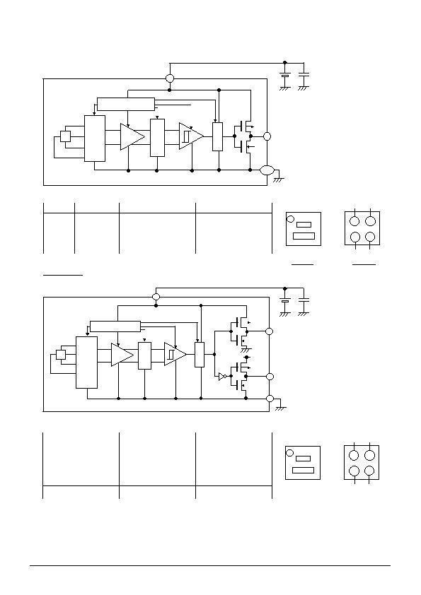
螧lock Diagram
BU52054GWZ, BU52055GWZ
PIN No.
PIN NAME
FUNCTION
COMMENT
A1
GND
GROUND
A2
GND
GROUND
B1
VDD
POWER SUPPLY
B2
OUT
OUTPUT
BU52015GUL
Fig.59
PIN No.
PIN NAME
FUNCTION
COMMENT
A1
OUT1
Output pin (Active Low)
A2
OUT2
Output pin (Active High)
B1
GND
GROUND
B2
VDD
Power Supply Voltage
OUT
GND
VDD
TIMING LOGIC
?
HALL
ELEMENT
B2
B1
Fig.58
Adjust the bypass capacitor
value as necessary, according
to voltage noise conditions, etc.
0.1礔
The CMOS output terminals enable direct
connection to the PC, with no external pull-up
resistor required.
0.1礔
A1
B2
B1
A2
Reverse
A2
B2
B1
A1
Surface
The CMOS output terminals enable direct
connection to the PC, with no external pull-up
resistor required.
Adjust the bypass capacitor value as
necessary, according to voltage noise
conditions, etc.
GND
OUT1
OUT2
VDD
GND
VDD
TIMING LOGIC
?
HALL
ELEMENT
A1
A2
B1
B2
A1
B2 B1
A2
Reverse
A2
B2
B1
A1
Surface
1,A2
发布紧急采购,3分钟左右您将得到回复。
相关PDF资料
BU52003GUL-E2
IC HALL EFFECT SW BIPO VCSP50L1
BU52014HFV-TR
IC HALL EFFECT SW BIPO HVSOF5
BU52040HFV-TR
IC HALL EFFECT BIPO LATCH HVSOF5
D6B-2P
SENSR TILT 35-65DEG 1MA SMD GUL
D7E-3
SENSOR TILT 50-80DEG 0.1A GRY
DSBA1H
SENSOR TILT SW 30-60DEG 20MA TH
EE-SA103
SENSOR OPTO SLOT 3MM TRANS THRU
EE-SA107-P2
OPTO SENSOR 3.6MM TRANS
相关代理商/技术参数
BU52002GUL
制造商:ROHM 制造商全称:Rohm 功能描述:Unipolar Detection Hall ICs
BU52002GUL_10
制造商:ROHM 制造商全称:Rohm 功能描述:Unipolar Detection Hall ICs
BU52002GUL_1008
制造商:ROHM 制造商全称:Rohm 功能描述:Unipolar Detection Hall ICs
BU52002GUL-E2
功能描述:板机接口霍耳效应/磁性传感器 Magnetic Sensor 2.4-3.3V; 50mS RoHS:否 制造商:Honeywell 类型:Bipolar Hall-Effect Digital Position Sensor 工作电源电压:3 V to 24 V 电源电流:3.5 mA 最大输出电流:20 mA 工作点最小值/最大值:5 G, 55 G 最小/最大释放点(Brp):- 55 G, - 5 G 最大工作温度:+ 150 C 安装风格:SMD/SMT 封装 / 箱体:SOT-23
BU52003GUL
制造商:ROHM 制造商全称:Rohm 功能描述:Unipolar Detection Hall ICs
BU52003GUL-E2
功能描述:板机接口霍耳效应/磁性传感器 Magnetic Sensor 2.4-3.3V; 50mS RoHS:否 制造商:Honeywell 类型:Bipolar Hall-Effect Digital Position Sensor 工作电源电压:3 V to 24 V 电源电流:3.5 mA 最大输出电流:20 mA 工作点最小值/最大值:5 G, 55 G 最小/最大释放点(Brp):- 55 G, - 5 G 最大工作温度:+ 150 C 安装风格:SMD/SMT 封装 / 箱体:SOT-23
BU52004GUL
制造商:ROHM 制造商全称:Rohm 功能描述:Hall effect Switch
BU52004GUL_10
制造商:ROHM 制造商全称:Rohm 功能描述:Omnipolar Detection Hall ICs (Polarity detection for both S and N features dual outputs)
